Computer Vision in Semiconductor Inspection
The semiconductor industry requires strict quality control at every stage of production, from the initial examination of silicon wafers to the final inspection of printed circuit boards. Machine vision has become a crucial technology in this sector, providing automated, high-speed, and very precise inspection capabilities that go beyond what human inspectors can achieve. By using industrial cameras, machine vision lenses, and powerful image processing methods, including deep learning, manufacturers can guarantee the quality and dependability of their semiconductor products throughout the entire manufacturing process. This article will discuss the important role of computer vision in semiconductor manufacturing, focusing on its uses from the detailed analysis of silicon wafers to the overall inspection of printed circuit boards.
Key areas where computer vision is significantly used include:
- Wafer Analysis: Identifying surface flaws, contamination, and structural problems on silicon wafers.
- Component Placement Verification: Ensuring that electronic components are placed correctly on PCBs.
- Solder Joint Inspection: Finding defects such as not enough solder, solder bridges, or cold solder joints.
- Deep Learning Integration: Using sophisticated algorithms for identifying and categorizing complex defects.
- PCB Inspection: Detecting manufacturing errors like missing components or incorrect positioning.
The ability of these systems to perform consistent and detailed inspections at high speeds directly contributes to increased yields, reduced waste, and ultimately, more dependable electronic products for consumers and industries alike.
Table of contents
Industrial Camera Selection for Semiconductor Inspection
Selecting the appropriate industrial camera is a fundamental step in designing an effective computer vision system for PCB inspection. The camera's specifications directly influence the quality of the captured images and, consequently, the accuracy of the defect detection process.
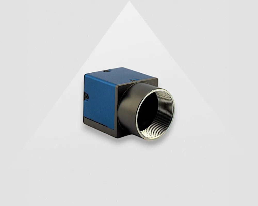
For still PCB inspection, we recommend the MER2-630-60U3C camera. This USB3 camera incorporates a Sony IMX178 sensor, providing a high resolution of 3088x2064 pixels. This high pixel count allows for the capture of fine details on the PCB, which is crucial for identifying small defects in components and solder joints.
The camera's ability to capture up to 60 frames per second ensures that images can be acquired quickly, facilitating efficient inspection workflows. The 1/1.8" sensor format offers a good balance between field of view and image quality.
The CMOS sensor technology contributes to the camera's high sensitivity and low noise characteristics, resulting in clear and detailed images. The colour capability of this camera allows for the identification of color coded components and potential discoloration defects on the PCB.
While the MER2-630-60U3C utilizes a rolling shutter, for still object inspection where motion blur is not a significant concern, this shutter type offers a cost-effective solution without compromising image quality for this specific application.

Selecting the Optimal Lens for Semiconductor Inspection
The selection of the appropriate machine vision lens is just as critical as the camera choice in building a robust computer vision system for PCB inspection. The lens determines the field of view, magnification, and image quality, all of which are essential for accurate defect detection.
For use with the MER2-630-60U3C camera in still PCB inspection, we recommend a C-Mount 12mm lens. The C-Mount interface ensures mechanical compatibility with the camera. A 12mm focal length provides a suitable field of view for inspecting sections of a PCB at a practical working distance, allowing for detailed examination of components and solder joints.
Maintaining low distortion is paramount in inspection applications, as any significant distortion can lead to inaccurate measurements and misidentification of defects. The recommended lens has a distortion level of less than 1%, which ensures that the captured images accurately represent the physical dimensions and shapes of the components on the PCB.
Selecting Proper Lighting for PCB Inspection
Appropriate machine vision lighting is paramount for obtaining clear and detailed images crucial for accurate PCB inspection.
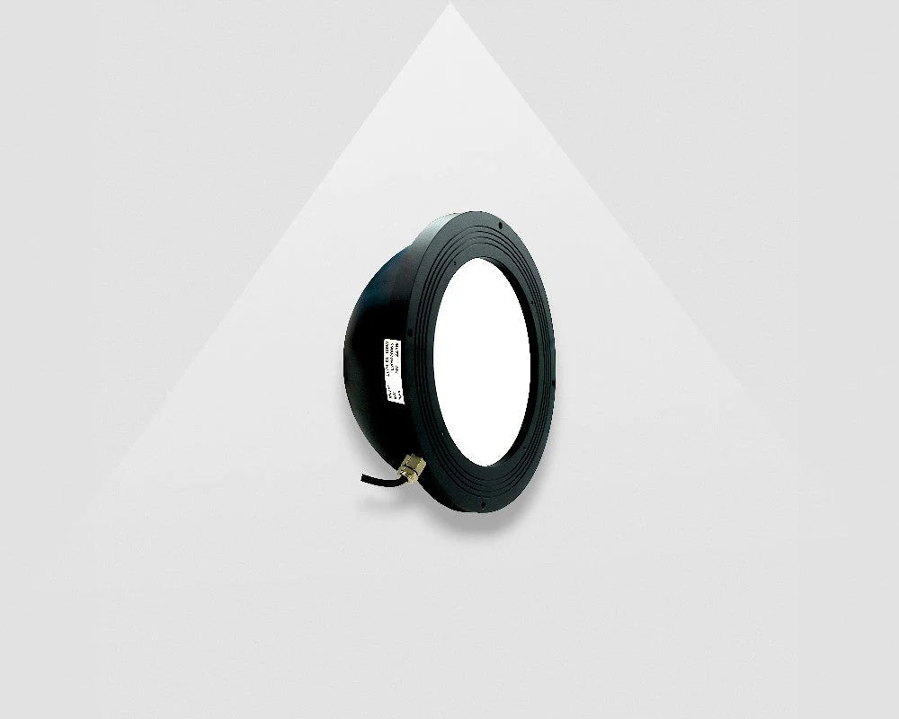
For PCB inspection, a dome light is often an excellent choice to avoid unwanted reflections. A dome light consists of an array of LEDs housed within a hemispherical enclosure. This design provides diffuse, even illumination from multiple angles, effectively reducing shadows and specular reflections from shiny surfaces like solder joints and component leads. By minimizing these reflections, a dome light allows the camera to capture a more uniform and detailed view of the PCB surface, making it easier to identify defects such as missing components, misalignments, or inconsistencies in solder joints.

Image Processing Software for PCB Inspection
For intricate tasks like PCB inspection, specialized software is essential to analyze the captured images and extract critical information about component placement, solder joint quality, and potential defects.
All our cameras are GenICam compatible, ensuring seamless integration with various image processing software platforms. This flexibility allows users to choose the software that best suits their needs and expertise. These include powerful vision libraries and development environments such as MvTec Halcon, NI LabVIEW, and Cognex Vision Pro, as well as more general-purpose platforms like MATLAB and OpenCV, providing users with a broad spectrum of tools to develop their inspection algorithms.
For users seeking a comprehensive software solution, Zebra Aurora Vision Studio is a highly recommended option. This robust yet intuitive software offers a visual programming interface, often likened to a toolbox, which simplifies the process of creating and deploying inspection applications. With Aurora Vision, users can implement a wide range of inspection tasks, including precise measurement of component dimensions, detection of missing or misaligned parts, and identification of various solder joint defects. The free Lite version of Aurora Vision, which includes a full suite of standard vision algorithms, serves as an excellent starting point for users to evaluate the software's capabilities and determine its suitability for their specific PCB inspection requirements.
Applications of Computer Vision in Semiconductor Inspection
Computer vision plays a vital role in numerous inspection stages throughout semiconductor manufacturing, from the initial wafer production to the final assembly of PCBs. Here are some key application examples:
These applications demonstrate the breadth and depth of how computer vision contributes to maintaining high quality standards and optimizing efficiency in the complex processes of semiconductor manufacturing.
Support for Computer Vision in Semiconductor Inspection
In summary, computer vision plays a big role in semiconductor manufacturing, ensuring high-quality production from wafer analysis to PCB inspection. Would you like to have support from one of our machine vision experts for creating your own semiconductor inspection system, from wafer analysis to PCB inspection? Or another similar vision system? Don’t hesitate to reach out by using the form below!


